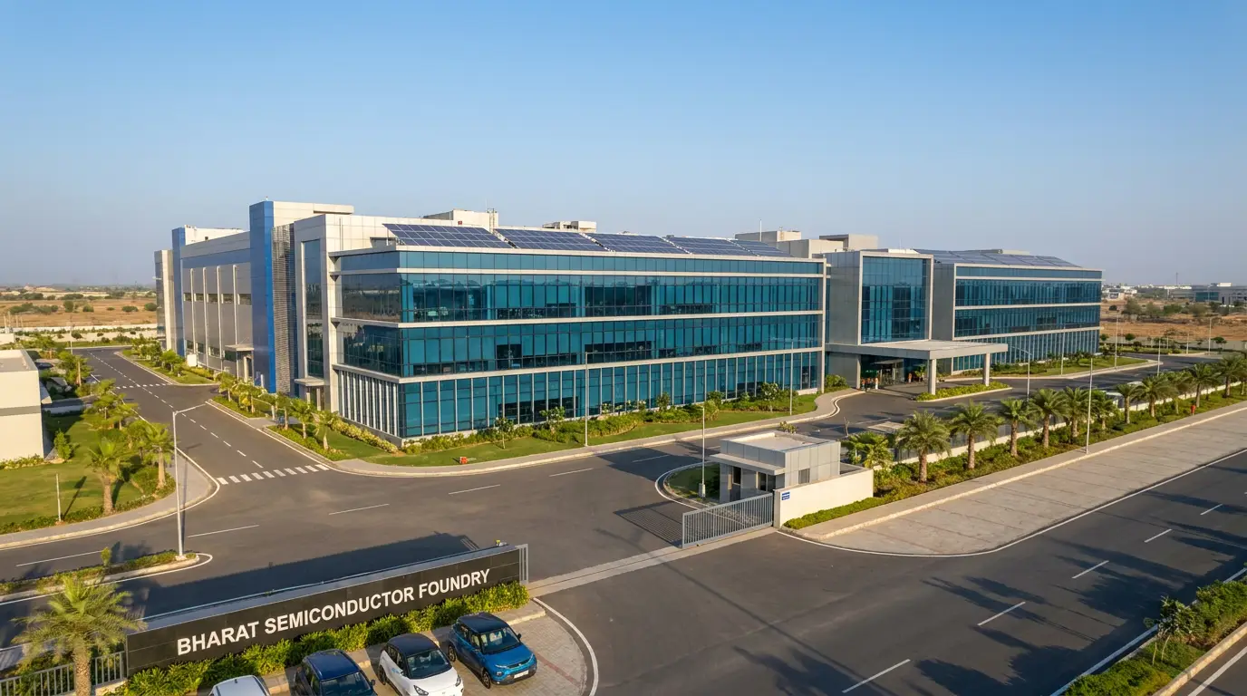
The Dholera semiconductor fab is India's first commercial chip fabrication plant, built by Tata Electronics with Taiwan's PSMC. The Union Cabinet approved it on 29 February 2024, and the foundation stone was laid on 13 March 2024. It is reported at an investment of up to about Rs 91,000 crore, with a target capacity of up to 50,000 wafers per month, under the India Semiconductor Mission. For Dholera SIR, it is the anchor that turned a plan into a national priority.
- Approved by the Union Cabinet on 29 February 2024
- Investment reported up to ~Rs 91,000 crore (~US$11 billion)
- Target capacity reported up to 50,000 wafers per month
- Reported to generate 20,000+ direct and indirect skilled jobs
Why this fab matters
For years, India designed chips but did not fabricate them at commercial scale at home. The Dholera fab is the project meant to change that. It is described as India's first commercial semiconductor fabrication plant, and it is being built inside Dholera SIR. That single fact reframes the whole region: Dholera stopped being just another planned city and became the home of a national-priority industry.
AskDholera is independent and does not sell plots. This guide lays out the verified facts about the fab and clearly marks anything that is reported or planned rather than confirmed.
The 2024 approval
The project reached a decisive milestone in early 2024. The Union Cabinet formally approved it on 29 February 2024. Shortly after, on 13 March 2024, Prime Minister Narendra Modi virtually laid the foundation stone for the fabrication plant. Those two dates are the anchor points of the fab's official timeline and mark the moment it moved from proposal to sanctioned project.
Tata Electronics and PSMC
The fab is being developed by Tata Electronics in partnership with Powerchip Semiconductor Manufacturing Corporation (PSMC) of Taiwan. The two completed a landmark agreement for technology transfer to build the fab, which is significant: it pairs Tata's manufacturing ambition and capital with an established foundry partner's process knowledge. For a country building its first commercial fab, that transfer of proven technology is one of the most important parts of the story.
Tata Electronics
The Indian promoter and operator, part of the Tata Group, driving the fab and a broader semiconductor ambition in India.
PSMC (Taiwan)
Powerchip Semiconductor Manufacturing Corporation, the technology partner, reported to provide process technology and know-how through a technology-transfer agreement.
Scale and capacity
The numbers are large, which is what makes the project a genuine anchor rather than a symbolic one. The fab is reported at an investment of up to about Rs 91,000 crore, roughly US$11 billion. It is reported to target a manufacturing capacity of up to 50,000 wafers per month, and to include next-generation factory automation using data analytics and machine learning for high factory efficiency.
As always, treat capacity and cost as reported and planned figures. They come from official and company announcements, but a fab ramps up over time, so real output builds gradually rather than switching on at full scale.
The India Semiconductor Mission
The Dholera fab was approved under the India Semiconductor Mission, the national programme designed to build domestic chip manufacturing capability. That framing matters for anyone reading the region's prospects: this is not a standalone private bet, it is part of a coordinated national strategy with central backing. A project inside a government mission tends to carry more policy support and long-term commitment than a purely commercial venture would on its own.
Jobs and skills
The employment story is a big part of why the fab reshapes Dholera. The project is reported to be expected to generate over 20,000 direct and indirect skilled jobs. Beyond this single fab, Tata Group's broader multi-fab vision for Dholera is reported to target more than 1,00,000 skilled jobs over the long term. These are planned figures tied to a phased build, so they arrive over years, not at once.
Skilled employment at that scale does more than fill one factory. It creates demand for housing, services, training and supporting businesses, which is exactly the kind of demand that reshapes a region around a single anchor industry.
The ripple on the region
A fab of this size does not sit in isolation. It tends to pull in a supporting ecosystem: suppliers, chemicals and gases, logistics, testing and packaging partners, and the housing and services that a large skilled workforce needs. The fab is reported to sit within the TP2 zone of Dholera SIR, one of the more developed parts of the region, which places it close to trunk infrastructure like roads, power and water.
For the wider region, the fab acts as proof of intent. It is one reason connectivity projects like the Ahmedabad-Dholera Expressway and the Dholera International Airport carry weight: heavy industry needs fast movement of people and goods. If you are weighing what this means for land, read our plot prices guide for how prices actually behave, and remember that an anchor project is a long-term tailwind, not a guarantee on any single plot. To choose who to deal with, start with the neutral developer guide.
Frequently asked questions
What is the Dholera semiconductor fab?
It is India's first commercial semiconductor fabrication plant, built in Dholera SIR by Tata Electronics with PSMC of Taiwan. It was approved by the Union Cabinet on 29 February 2024 under the India Semiconductor Mission.
How big is the investment?
It is reported at an investment of up to about Rs 91,000 crore, roughly US$11 billion, with a target capacity of up to 50,000 wafers per month.
How many jobs will it create?
The fab is reported to be expected to create over 20,000 direct and indirect skilled jobs. Tata Group's broader multi-fab vision for Dholera is reported to target more than 1,00,000 skilled jobs over the long term. These are planned figures.
When did construction start?
The foundation stone was laid on 13 March 2024. As of mid-2026, major structural work is reported complete with cleanroom and equipment installation reported underway. A confirmed date for first commercial chip production should be verified from official sources.